| Ceramic PCB Process Capability |
| Project | Thick film ceramic board process capabilities | DBC/DCB Copper Copy Ceramics Square Process Capability | DPC direct copper plating ceramic substrate process capacity | AMB activated metal welding ceramic substrate |
| Number of circuit layers | 10 layer | 2 layer | 2 layer | 2 layer |
| Biggest size | 200*200mm | 138*178mm | 138*190mm | 114*114mm |
| Minimum board thickness | 0.25mm | 0.30mm~0.40mm | 0.25mm | 0.25mm |
| Maximum board thickness | 2.0mm | 1L: 1.3mm; 2L: 1.6mm | 2.0mm | 1.8mm |
| Conductor thickness | 5um-13um | 3.9oz-8.6oz | 2um-200um | 8oz-22.9oz |
| Minimum line width/line distance | 6/8mil (0.15/0.20mm) | 12/12mil (0.30/0.30mm) | 6/8mil (0.15/0.20mm) | 20/20mil (0.50/0.50mm) |
| Substrate | One aluminum, aluminum nitride, oxidation, oxide | Alumina, aluminum nitride, oxide | Alumina, aluminum nitride, oxide, silicon nitride | Aluminum nitride, silicon nitride |
| Base material | 0.25, 0.38, 0.50, 0.635, 0.80, 1.0, 1.25, 1.5, 2.0mm | 0.25, 0.38, 0.50, 0.635, 0.76, 1.0mm | 0.25, 0.38, 0.50, 0.635, 0.80, 1.0, 1.25, 1.5, 2.0mm | 0.25, 0.38, 0.50, 0.635, 0.76, 1.0mm |
| Minimum | 4mil (0.1mm) | |||
| Minimum hole distance | NPTH: 16mil (0.30mm); PTH: 20mil (0.5mm) | |||
| Minimum PAD ring (single) | 6mil(0.15mm) | N/A | 3mil(0.075mm) | N/A |
| PTH minimum hole wall copper thickness | 4mil(10um) | N/A | 4mil (10um) | N/A |
| Welding pad minor diameter | 10mil(0.25mm) | 8mil(0.20mm) | 6mil(0.15mm) | 8mil(0.20mm) |
| Group welding bridge | 12mil(0.30mm) | 8mil(0.20mm) | 6mil(0.15mm) | 8mil(0.20mm) |
| BGA pads minimum spacing | 12mil(0.30mm) | 8mil(0.20mm) | 5mil(0.125mm) | 8mil(0.20mm) |
| PTH/NPTH pore diameter tolerance | PTH: ±4mil (0.1mm) ; NPTH: ±2mil (0.05mm) | |||
| Pole bias tolerance | ± 4mil (0.1mm) | |||
| Tolerance | Laser cutting: +0.2/0.05mm; Mold type type: +0.25/0.20mm | Laser cutting: +0.2/0.05mm | Laser cutting: +0.2/0.05mm; Mold type type: +0.25/0.20mm | Laser cutting: +0.2/0.05mm |
| Line width/line distance tolerance | ± 5mil (0.125mm) | ± 5mil (0.125mm) | ± 1mil (0.025mm) | ± 5mil (0.125mm) |
| Surface treatment | AgPd, AuPd, Mn/Ni | OSP ,ENIG ,ENEPIG etc | OSP ,ENIG,ENEPIG etc | OSP ,ENIG, ENEPIG etc |
| Thermal Stress | 1 hour @ 350℃ | 3 x 10 Sec @ 280 ℃ | 15 min @ 350 ℃ | 3 x 10 Sec @ 280 ℃ |
FAQ
Q1: What’s your minimum order quantity?
A1: We have no MOQ ,1pcs is welcomed.
Q2: What file we should offer?
A2: PCB:Gerber file is better, ( Protel, power pcb, PADs file),
PCBA: Gerber file and BOM list.
Q3: No PCB file/GBR file, only have the PCB sample, can you produce it for me?
A3: Yes, we could help you to clone the PCB. Just send the sample PCB to us, we could clone the PCB design and work out it.
Q4: What any other information should be offered except for file?
A4:Following specifications are needed for quotation:
a) Base material
b) Board thickness:
c) Copper thickness
d) Surface treatment:
e) color of solder mask and silkscreen
f) Quantity
Q5:I am very satisfied after I read your information, how can I start to purchase my order?
A5: You could send your file to requirements to our email : sales@toprightpcb.com
Q6 : What’s your payment type ?
A6: TT , Western Union , Paypal , Alipay etc
Q7: What is delivery terms and time?
A7: We usually use FOB terms and ship the PCBs in 5-15 workdays depending on your order quantity.
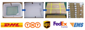
Q8: What is your packaging and shipment type ?
A8: